
RF is the abbreviation of Radio Frequency. It means the electromagnetic frequency that can be radiation to space, and the frequency range is from 300kHz to 300GHz. RF is radio frequency current, RF in short. It is the abbreviation of a high-frequency AC variation electromagnetic wave.
The alternating current that changes less than 1000 times per second is called low-frequency current, and the one that changes more than 10000 times is called high-frequency current. And RF is such a high-frequency current. Radio frequency (300K-300G) is the higher frequency band of high frequency (greater than 10K). Microwave band (300M-300G) is also the higher frequency band of RF.
01
Q: I would like to ask a question about the peak-to-average ratio and PA power selection. Assuming that the output peak-to-average ratio of the source modulated signal is 10dB, and the amplifier is designed to amplify this signal. Is it OK to align the P1dB value of the amplifier device with the corresponding peak power of the modulated signal after amplification? GaN many are not given P1dB, are given a Psat (P3dB), a little worried about the peak signal distortion.
A: Is there a specific modulation limit for Psat that does not give OP1dB, such as GFSK?
A: No, many GaN amplifiers are given Psat. Its P1dB and LDMOS P1dB curve is different, the measured output is very small signal may be compressed by 1dB. And then push the high power is also compressed by 1dB, until near saturation power will appear further compression.
Some high-order modulation signal peak-to-average ratio requirements. I would have trouble with this consideration when selecting a model. I am a little worried that the design is not enough and the error code cannot be solved later.
A: GaN this compression characteristic is saturated output to be quite a bit larger than P1dB. And choose the right operating point to have a better linearity.
Q: So it is still necessary to choose the appropriate bias point, so that P1dB and Psat are similar to the real use? If in the small signal has been compressed 1dB, the signal must have been distorted, then how to solve it?
A: This is relevant to the specific application. Applied to the base station, the system DPD correction capability is strong, the power from P3dB on backward just Terminal class application system DPD correction ability is weak, or no DPD, it requires the PA itself to have good linearity, and the power generally starts to fall back from P1dB.
A: For GaN, its application is generally on the base station side. The system DPD capability is strong, so the PA device of the base station only needs to be responsible for two things: one is to generate enough power; the other is to have better efficiency when the power is large enough. Both of these are strong points of GaN. As for the P1dB forward, the impact is only linearity, as long as the system DPD can be calibrated back is not a problem.
02
Q: Can you tell me how to consider the thermal effect generation in simulation when using GaAs HBT for PA design? The previous design had gain collapse at high bias for small signals and gain collapse at large signals.
For example, if the load line has entered the non-safety zone under large signal, how to notice it in the simulation? Or is there an empirical value for the value of the base ballast resistor?
A: Gain collapse is relevant to the selection of bias voltage and ballast resistor values. You can adjust the bias voltage a little bit smaller to make the PA Beta value before the highest point of its curve at large signals.
Q: Is it possible to observe vbe at large signal and compare the curve of β with vbe.
A: PDK has beta and vbe curves inside, so you can know the vbe value corresponding to the beta inflection point; use ads to simulate the gm template.
Q: Thanks, I understand. And what is the approximate range for the size of the ballast resistor?
A: HBT general and tube area product not less than 60000 , but also to see the two-tone IMD3 characteristics, will go to optimize this value. Also and the output power, overcurrent capacity related to it, or their own tuning, this is not very well set.
03
Q: When I do the CW test with R&S, I can’t see anything except the output power. Is it because the source is not set right?
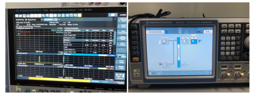
A: Without modulation, the monophonic signal does not contain information, and you cannot see the EVM.
04
Q: I would like to ask the multi-stage amplifier generally assign the front stage gain is large, the rear stage gain is small. What is the reason for this?
A: My understanding is that if it is a PA, the rear stage is used to do the final power amplification and drive the 50 ohm load. This time to do the matching is often the maximum power matching, can not achieve maximum gain. So the realization of gain has to rely more on the front stage. If it is LNA, from the noise factor cascade formula is easy to understand. The front stage gain to do a large, the noise contribution of the rear stage will be small.
A: There is another reason is that the rear stage is generally larger tube size, larger parasitic capacitance, the maximum available gain is relatively low. This is also the reason why the gain of the rear stage is difficult to do up.
05
Q: Please tell me why MAG has this trend changed?
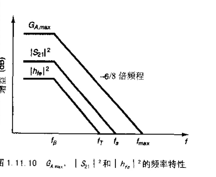
A: Because there are Cgs and Cgd.
A: You consider the first-order equivalent circuit of the tube together with the gate source capacitance, and then write the gain expression is this. See Microwave Engineering specifically, the cutoff frequency is a function of the gate source capacitance, so say 6dB octave.
Q: The question I want to ask is whether there is a range of frequencies, large enough to be this trend, at low frequencies?
A: The low frequency actually decreases, the cross-conductance remains the same so that the low frequency is a horizontal line. Low frequency does not take into account the capacitance, the gain is only related to the cross-conductance and load.
A: You can deduce it step by step according to the definition of several gains. Get the formula and understand it naturally. Derivation once helps to understand the circuit and the conclusion.
Simply look at it can be thought of this way: because the circuit has a capacitor, the high-frequency gain decreases. Guessing that the gain is positively related to the impedance of a certain capacitor (capacitor’s high-frequency impedance = picture). Because the derivation is a linear gain, the initial thought is that there is no second-order or higher-order sources. Guessing and the first-order impedance of the capacitor is proportional. That is the picture.
For this gain formula above, the frequency doubles, and the gain decreases by 1/2. For voltage or current gain, use 20log to calculate. So when the frequency is doubled, the gain is reduced by 20*log(1/2)=-6dB. I.e.: the frequency is increased by one octave, and the gain is reduced by 6dB.
Although the above is to look at the answer to the conclusion, but the general idea on the right, there is no need to entangle too much.
In addition, there is a High Light point of attention here, the translation of the figure has a major error, which is -6dB per octave (some books write -20dB per 10 octave, is the same thing), rather than -6dB per 8 octave, may have caused a tangle here. The original book says “Octave”, many Chinese translations into 8 times, which is incorrect. “Octave” is the “octave” in the musical scale, an “octave” is a major key, containing “Do re mi fa so la si” seven main notes, doubling the frequency between adjacent octaves and octaves. So an “Octave” means one octave, not eight octaves.
Below is a screenshot from Microwave TransistorAmplifiers (Guillermo Gonzalez) for reference.
(Image taken from Microwave TransistorAmplifiers, Guillermo Gonzalez)
06
Q: I would like to ask the HBT PA output network Q value, in addition to the impact of bandwidth, what other effects ah?
A: Considering the loss, definitely the power efficiency are affected.
A: For a matched network, the Q value of the network affects the loss. It can be deduced that the loss of a matching network is proportional to the network Q, and the device Q (mainly inductance) is inversely proportional, that is:
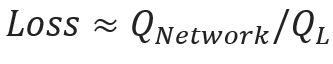
So after the network Q value increases, the output matching loss increases. The efficiency and power will fall down.
07
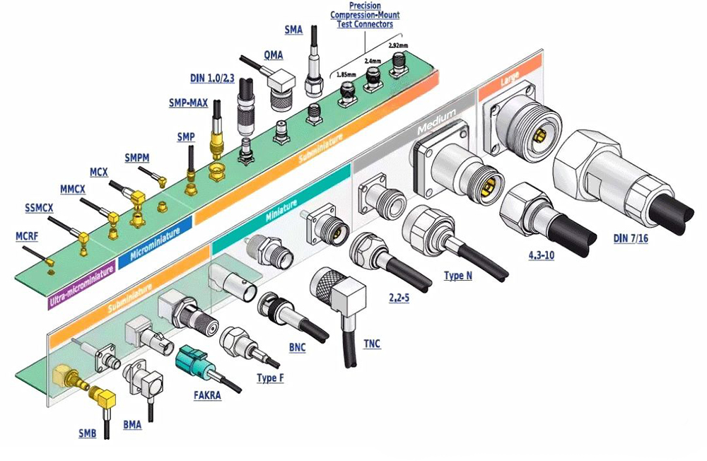
Q: I would like to ask what type of RF head is this SMA to, and what is the official scientific name? Thanks.
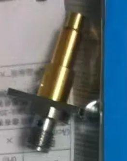
A:You can refer to the name marked in the chart below.
08
Q: I would like to ask, why does the npn tube turn on automatically if it does not give a base bias potential?
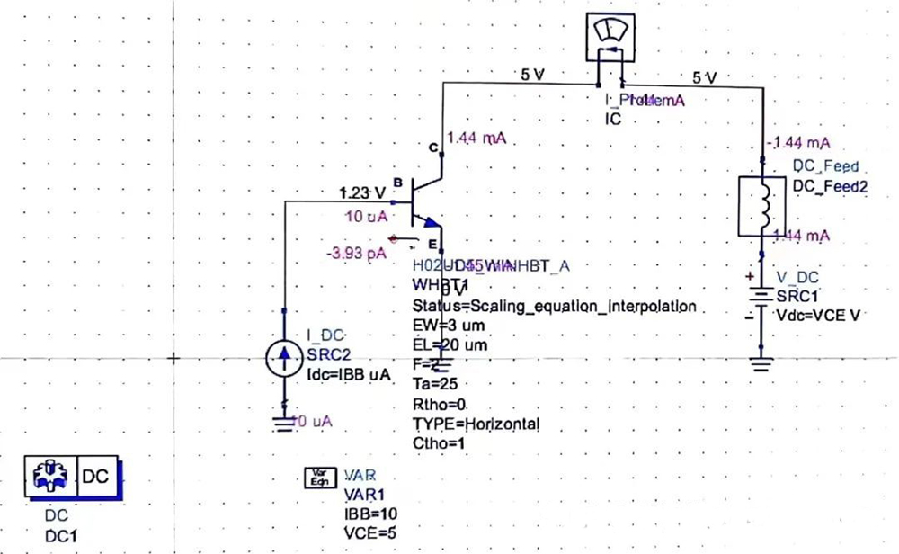
A: Current-driven tube is turned on.
A: The BASE voltage is built up with the current source driving. Look at the diagram Vb voltage has reached 1.23V.